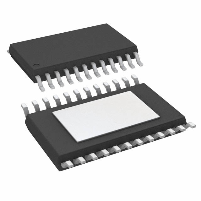
Texas Instruments CDCVF2509PW

| Quantity | Unit Price | Total Price |
|---|---|---|
| 1 | $33.80 | $33.80 |
| 15+ | $7.77 | $116.55 |
| 25+ | $7.61 | $190.25 |
| 50+ | $7.18 | $359.00 |
| 100+ | $6.34 | $634.00 |
| N+ | $1.27 | Price Inquiry |
Request Quote / Inquiry
| Product attributes | Property Value |
| Manufacturer | Texas Instruments |
| Product Series | |
| Packaging | Marketplace | Tube |
| Type | PLL Clock Driver |
| PLL | Yes with Bypass |
| Input | LVTTL |
| Output | LVTTL |
| Number of Circuits | 1 |
| Ratio - Input:Output | 2:10 |
| Differential - Input:Output | No/No |
| Frequency - Max | 175MHz |
| Divider/Multiplier | No/No |
| Voltage - Supply | 3V ~ 3.6V |
| Operating Temperature | 0°C ~ 85°C |
| Grade | - |
| Qualification | - |
| Mounting Type | Surface Mount |
| Package / Case | 24-TSSOP (0.173", 4.40mm Width) |
| Supplier Device Package | 24-TSSOP |
| ROHS |  |
The CDCVF2509PW from Texas Instruments is a PLL Clock Driver with a single circuit, designed for high-performance clock distribution. It supports frequencies up to 175MHz with LVTTL inputs and outputs, and includes a bypassable PLL for flexible operation. Housed in a 24-TSSOP package, it operates from 0°C to 85°C, making it ideal for DDR memory, networking, and telecom applications.
- High Frequency Support: Handles up to 175MHz, suitable for modern high-speed digital systems.
- PLL Bypass Option: Provides flexibility to use the device as a simple buffer when PLL is not needed.
- LVTTL Compatibility: Works with standard 3.3V logic, simplifying power supply design.
- Low Skew Distribution: Ensures minimal delay differences between output clocks, critical for parallel interfaces.
DDR Memory Clock Distribution
The CDCVF2509PW provides low-skew LVTTL clocks for DDR memory modules, ensuring precise timing for data strobes.
Networking Switch Timing
Distribute a clean 175MHz clock to multiple PHY chips, maintaining synchronization in high-speed Ethernet switches.
Processor Reference Clock
Generate a stable reference clock for FPGAs and ASICs, reducing jitter and improving system reliability.
Telecom Line Cards
Use the PLL to clean and distribute clocks across line cards, ensuring consistent framing and data alignment.
Broadcast Video Equipment
Synchronize video processing chips to a common clock, preventing frame drops and artifacts.
Industrial Computing
Provide a reliable clock for embedded PCs and controllers, enhancing deterministic operation.
- Q: What type of device is the CDCVF2509PW?
- A: It is a PLL Clock Driver, designed to distribute and synchronize clock signals.
- Q: Does it support PLL bypass?
- A: Yes, the PLL can be bypassed, allowing direct clock distribution without phase locking.
- Q: What are the input and output types?
- A: Both input and output are LVTTL, compatible with 3.3V logic levels.
- Q: How many circuits does it have?
- A: It contains 1 circuit.
- Q: What is the maximum frequency?
- A: The CDCVF2509PW supports up to 175MHz.
- Q: What is the package and temperature range?
- A: It comes in a 24-TSSOP package and operates from 0°C to 85°C.
 CDCVF2509PW.pdf
- Q: What type of device is the CDCVF2509PW?
- A: It is a PLL Clock Driver, designed to distribute and synchronize clock signals.
- Q: Does it support PLL bypass?
- A: Yes, the PLL can be bypassed, allowing direct clock distribution without phase locking.
- Q: What are the input and output types?
- A: Both input and output are LVTTL, compatible with 3.3V logic levels.
- Q: How many circuits does it have?
- A: It contains 1 circuit.
- Q: What is the maximum frequency?
- A: The CDCVF2509PW supports up to 175MHz.
- Q: What is the package and temperature range?
- A: It comes in a 24-TSSOP package and operates from 0°C to 85°C.