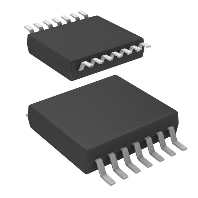
Texas Instruments SN74LVC126ADGVR

| Quantity | Unit Price | Total Price |
|---|---|---|
| 1 | $0.33 | $0.33 |
| 15+ | $0.32 | $4.80 |
| 25+ | $0.32 | $8.00 |
| 50+ | $0.30 | $15.00 |
| 100+ | $0.26 | $26.00 |
| N+ | $0.05 | Price Inquiry |
Request Quote / Inquiry
| Product attributes | Property Value |
| Manufacturer | Texas Instruments |
| Product Series | 74LVC |
| Packaging | Cut Tape (CT) | Tape & Reel (TR) |
| Part Status | Active |
| Logic Type | Buffer, Non-Inverting |
| Number of Elements | 4 |
| Number of Bits per Element | 1 |
| Input Type | - |
| Output Type | 3-State |
| Current - Output High, Low | 24mA, 24mA |
| Voltage - Supply | 1.65V ~ 3.6V |
| Operating Temperature | -40°C ~ 125°C (TA) |
| Grade | - |
| Qualification | - |
| Mounting Type | Surface Mount |
| Package / Case | 14-TFSOP (0.173", 4.40mm Width) |
| Supplier Device Package | 14-TVSOP |
| ROHS |  |
The SN74LVC126ADGVR from Texas Instruments is a quad non-inverting buffer with 3-State outputs, designed for low-voltage, high-speed applications. Operating from 1.65V to 3.6V, it provides 24mA of drive current per channel, ensuring robust signal delivery. The 14-pin TFSOP package is compact and suitable for dense PCB layouts. This buffer is ideal for bus interfacing, level shifting, and signal buffering in 1.8V to 3.3V systems.
- High Drive Current (24mA): Drives heavy capacitive loads and long traces with minimal signal degradation.
- Wide 1.65V to 3.6V Supply Range: Compatible with 1.8V and 3.3V logic, simplifying mixed-voltage designs.
- Low Propagation Delay: Ensures high-speed operation suitable for modern digital interfaces.
- 3-State Outputs: Provides bus isolation and prevents contention in multi-device systems.
High-Speed Bus Driving
With 24mA output drive, the SN74LVC126A can drive heavily loaded buses with fast edge rates, making it suitable for high-speed digital systems like DDR memory interfaces.
Level Shifting Between 1.8V and 3.3V
The 1.65V to 3.6V supply range allows seamless translation between low-voltage processors (1.8V) and 3.3V peripherals, preserving signal integrity.
FPGA/CPLD Signal Buffering
Buffer outputs from FPGAs to drive external components or long PCB traces. The 3-State feature enables multiple FPGA pins to share a common bus.
Server and Networking Equipment
In data centers, this buffer drives control and data lines across backplanes. The high drive current and low propagation delay ensure reliable operation at high frequencies.
Test and Measurement Instruments
Use the buffer to isolate measurement circuits from the device under test (DUT). The 3-State output allows the instrument to be disconnected when not in use.
Consumer Electronics Interfaces
Buffer signals in set-top boxes, gaming consoles, and smart TVs. The low-voltage operation reduces power consumption while maintaining high performance.
- Q: What logic family does the SN74LVC126ADGVR belong to?
- A: It is part of the 74LVC (Low-Voltage CMOS) family, known for high speed and low power at 3.3V.
- Q: What is the function of this IC?
- A: It is a quad (4-channel) non-inverting buffer with 3-State outputs, ideal for bus driving.
- Q: How many channels does it have?
- A: It contains 4 independent buffer channels, each with its own output enable control.
- Q: What is the output type?
- A: The outputs are 3-State, allowing high, low, or high-impedance states for bus isolation.
- Q: What is the operating voltage range?
- A: It operates from 1.65V to 3.6V, supporting both 1.8V and 3.3V logic systems.
- Q: What package is available?
- A: It is available in a 14-pin TFSOP package (0.173", 4.40mm width).
 SN74LVC126ADGVR.pdf
- Q: What logic family does the SN74LVC126ADGVR belong to?
- A: It is part of the 74LVC (Low-Voltage CMOS) family, known for high speed and low power at 3.3V.
- Q: What is the function of this IC?
- A: It is a quad (4-channel) non-inverting buffer with 3-State outputs, ideal for bus driving.
- Q: How many channels does it have?
- A: It contains 4 independent buffer channels, each with its own output enable control.
- Q: What is the output type?
- A: The outputs are 3-State, allowing high, low, or high-impedance states for bus isolation.
- Q: What is the operating voltage range?
- A: It operates from 1.65V to 3.6V, supporting both 1.8V and 3.3V logic systems.
- Q: What package is available?
- A: It is available in a 14-pin TFSOP package (0.173", 4.40mm width).