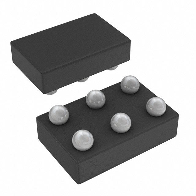
Texas Instruments SN74LVC2G34YZPR

| Quantity | Unit Price | Total Price |
|---|---|---|
| 1 | $0.71 | $0.71 |
| 15+ | $0.69 | $10.35 |
| 25+ | $0.68 | $17.00 |
| 50+ | $0.64 | $32.00 |
| 100+ | $0.56 | $56.00 |
| N+ | $0.11 | Price Inquiry |
Request Quote / Inquiry
| Product attributes | Property Value |
| Manufacturer | Texas Instruments |
| Product Series | 74LVC |
| Packaging | Marketplace | Cut Tape (CT) |
| Part Status | Active |
| Logic Type | Buffer, Non-Inverting |
| Number of Elements | 2 |
| Number of Bits per Element | 1 |
| Input Type | - |
| Output Type | Push-Pull |
| Current - Output High, Low | 32mA, 32mA |
| Voltage - Supply | 1.65V ~ 5.5V |
| Operating Temperature | -40°C ~ 85°C (TA) |
| Grade | - |
| Qualification | - |
| Mounting Type | Surface Mount |
| Package / Case | 6-XFBGA, DSBGA |
| Supplier Device Package | 6-DSBGA |
| ROHS |  |
The SN74LVC2G34YZPR from Texas Instruments is a dual non-inverting buffer designed for low-voltage applications. Operating from 1.65V to 5.5V, it provides 32mA source and sink current, ensuring robust signal drive. The push-pull outputs eliminate the need for external pull-up resistors, simplifying design. Its 2 channels are ideal for buffering clocks, reset lines, or control signals. Housed in a compact 6-XFBGA package, it is perfect for space-constrained, battery-powered devices.
- Wide 1.65V to 5.5V Supply Range: Compatible with 1.8V, 2.5V, and 3.3V systems, reducing design complexity.
- Push-Pull Outputs: Provide clean signal edges without external components, saving board space.
- Ultra-Small DSBGA Package: Ideal for miniaturized IoT and wearable designs.
- High Drive Current (32mA): Ensures reliable signal integrity even with capacitive loads.
Level Shifting for I2C and SPI
Use the SN74LVC2G34 to buffer and level-shift I2C or SPI signals between 1.8V sensors and 3.3V microcontrollers. The wide voltage range ensures compatibility without external level shifters.
Clock Signal Buffering
In portable devices, buffer clock signals to multiple peripherals. The push-pull output provides clean edges, reducing jitter and ensuring reliable timing.
GPIO Expansion and Isolation
Isolate a microcontroller's GPIO pins from external loads. The buffer prevents back-voltage spikes from damaging the MCU, while providing additional drive current.
Battery-Powered IoT Nodes
For low-power IoT sensors, this buffer operates down to 1.65V, preserving battery life. Its small DSBGA package fits into compact PCB layouts.
Wearable Device Signal Conditioning
In wearables, buffer signals from flex sensors or heart-rate monitors. The low-voltage operation reduces power consumption, extending battery life.
FPGA Configuration Interfacing
Buffer configuration signals between an FPGA and configuration memory. The push-pull outputs drive the memory's inputs reliably at 1.8V or 2.5V.
- Q: What logic family does the SN74LVC2G34YZPR belong to?
- A: It is part of the 74LVC family, known for low-voltage operation and high-speed.
- Q: What is the function of this IC?
- A: It is a dual buffer with non-inverting outputs, used for signal buffering and fan-out.
- Q: How many channels are available?
- A: It has 2 independent channels, each providing a single buffer stage.
- Q: What is the output type?
- A: The outputs are Push-Pull, providing strong drive without the need for pull-up resistors.
- Q: What is the voltage range?
- A: It operates from 1.65V to 5.5V, supporting both 1.8V and 3.3V logic levels.
- Q: What package is used?
- A: It comes in a 6-XFBGA (DSBGA) package, ideal for space-constrained designs.
 SN74LVC2G34YZPR.pdf
- Q: What logic family does the SN74LVC2G34YZPR belong to?
- A: It is part of the 74LVC family, known for low-voltage operation and high-speed.
- Q: What is the function of this IC?
- A: It is a dual buffer with non-inverting outputs, used for signal buffering and fan-out.
- Q: How many channels are available?
- A: It has 2 independent channels, each providing a single buffer stage.
- Q: What is the output type?
- A: The outputs are Push-Pull, providing strong drive without the need for pull-up resistors.
- Q: What is the voltage range?
- A: It operates from 1.65V to 5.5V, supporting both 1.8V and 3.3V logic levels.
- Q: What package is used?
- A: It comes in a 6-XFBGA (DSBGA) package, ideal for space-constrained designs.