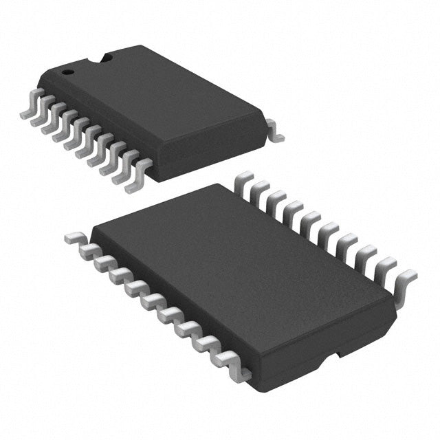
Texas Instruments SN74LVT244BDW

| Quantity | Unit Price | Total Price |
|---|---|---|
| 1 | $0.96 | $0.96 |
| 15+ | $0.93 | $13.95 |
| 25+ | $0.91 | $22.75 |
| 50+ | $0.86 | $43.00 |
| 100+ | $0.76 | $76.00 |
| N+ | $0.15 | Price Inquiry |
Request Quote / Inquiry
| Product attributes | Property Value |
| Manufacturer | Texas Instruments |
| Product Series | 74LVT |
| Packaging | Marketplace | Tube |
| Part Status | Active |
| Logic Type | Buffer, Non-Inverting |
| Number of Elements | 2 |
| Number of Bits per Element | 4 |
| Input Type | - |
| Output Type | 3-State |
| Current - Output High, Low | 32mA, 64mA |
| Voltage - Supply | 2.7V ~ 3.6V |
| Operating Temperature | -40°C ~ 85°C (TA) |
| Grade | - |
| Qualification | - |
| Mounting Type | Surface Mount |
| Package / Case | 20-SOIC (0.295", 7.50mm Width) |
| Supplier Device Package | 20-SOIC |
| ROHS |  |
The SN74LVT244BDW from Texas Instruments is a dual non-inverting buffer with 3-State outputs, part of the 74LVT BiCMOS family. It operates from 2.7V to 3.6V and delivers 32mA sink / 64mA source current, making it ideal for high-capacitance bus applications. The 20-pin SOIC package is suitable for a wide range of industrial and telecom designs. Its high drive strength and low propagation delay ensure reliable performance in demanding systems.
- High Drive Current (32mA/64mA): Drives heavy capacitive loads and long buses without signal degradation.
- Wide 2.7V to 3.6V Supply: Optimized for 3.3V systems with margin for voltage variations.
- 3-State Outputs: Enables bus sharing and reduces power consumption when idle.
- BiCMOS Technology: Combines low power of CMOS with high speed of bipolar for superior performance.
- Industrial Temperature Range: Reliable from -40°C to 85°C for harsh environments.
High-Drive Bus Buffering
With 32mA sink and 64mA source capability, the SN74LVT244BDW can drive heavily loaded backplanes or memory buses with excellent noise margins, reducing the need for additional driver stages.
3.3V Telecom Line Cards
In telecom equipment, use this buffer to interface between line interface units and switching ASICs. The high drive current ensures reliable data transmission over long PCB traces.
Memory Address/Data Buffering
Buffer address and data lines between a 3.3V DRAM controller and multiple memory modules. The 3-State outputs allow the controller to release the bus during refresh cycles.
Level Shifting (5V to 3.3V)
Although designed for 3.3V, the 5V-tolerant inputs (if supported) allow interfacing with legacy 5V logic, simplifying mixed-voltage system design.
Industrial PLC I/O Modules
Drive optocouplers or relay drivers in programmable logic controllers. The high current capability and wide temperature range (-40°C to 85°C) ensure robust operation in factory environments.
Server Motherboard Clock Distribution
Buffer clock signals to multiple loads (e.g., DIMMs, PCIe slots) with minimal skew. The 3-State feature allows clock gating for power management.
- Q: What logic family is the SN74LVT244BDW?
- A: It belongs to the 74LVT family, which is a BiCMOS logic family designed for low-voltage, high-drive applications.
- Q: What is the function of this device?
- A: It is a dual (2-channel) non-inverting buffer with 3-State outputs, used for bus driving and signal buffering.
- Q: How many channels are available?
- A: It has 2 independent buffer channels, each with its own output enable control.
- Q: What is the output type?
- A: The outputs are 3-State, allowing them to be placed in a high-impedance state for bus multiplexing.
- Q: What is the voltage range?
- A: It operates from 2.7V to 3.6V, optimized for 3.3V systems.
- Q: What package does it come in?
- A: It is available in a 20-pin SOIC package (7.50mm width), suitable for through-hole or surface-mount assembly.
 SN74LVT244BDW.pdf
- Q: What logic family is the SN74LVT244BDW?
- A: It belongs to the 74LVT family, which is a BiCMOS logic family designed for low-voltage, high-drive applications.
- Q: What is the function of this device?
- A: It is a dual (2-channel) non-inverting buffer with 3-State outputs, used for bus driving and signal buffering.
- Q: How many channels are available?
- A: It has 2 independent buffer channels, each with its own output enable control.
- Q: What is the output type?
- A: The outputs are 3-State, allowing them to be placed in a high-impedance state for bus multiplexing.
- Q: What is the voltage range?
- A: It operates from 2.7V to 3.6V, optimized for 3.3V systems.
- Q: What package does it come in?
- A: It is available in a 20-pin SOIC package (7.50mm width), suitable for through-hole or surface-mount assembly.