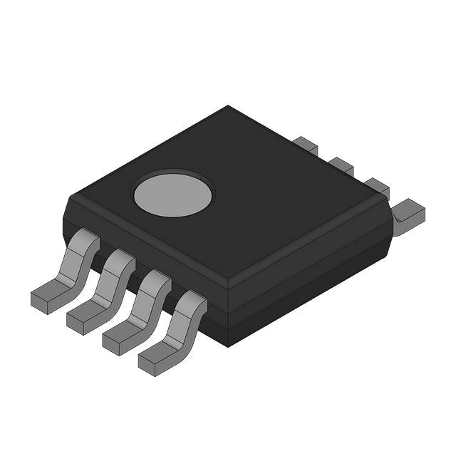
ADSANTEC ASNT8050-PQB

| Quantity | Unit Price | Total Price |
|---|---|---|
| 1 | $237.50 | $237.50 |
| 15+ | $230.00 | $3,450.00 |
| 25+ | $225.00 | $5,625.00 |
| 50+ | $212.50 | $10,625.00 |
| 100+ | $187.50 | $18,750.00 |
| N+ | $37.50 | Price Inquiry |
Request Quote / Inquiry
| Product attributes | Property Value |
| Manufacturer | ADSANTEC |
| Product Series | |
| Packaging | Bulk | |
| Type | PLL Clock Multiplier |
| PLL | Yes with Bypass |
| Input | CML, LVDS |
| Output | CML, LVDS |
| Number of Circuits | 1 |
| Ratio - Input:Output | 1:1 |
| Differential - Input:Output | Yes/Yes |
| Frequency - Max | 12.7GHz |
| Divider/Multiplier | Yes/Yes |
| Voltage - Supply | 3.1V ~ 3.5V |
| Operating Temperature | -25°C ~ 85°C |
| Grade | - |
| Qualification | - |
| Mounting Type | Surface Mount |
| Package / Case | 40-VFQFN Exposed Pad |
| Supplier Device Package | 40-QFN (6x6) |
| ROHS |  |
The ASNT8050-PQB from ADSANTEC is a PLL Clock Multiplier featuring a bypassable PLL for flexible operation. With 1 circuit and support for CML and LVDS inputs/outputs, it delivers up to 12.7 GHz output frequency. Its differential signaling ensures low noise and high signal integrity. Operating from -25°C to 85°C in a 40-VFQFN package, it is designed for high-speed networking, optical, and test applications.
- PLL Bypass Option: Offers flexibility to use external clock sources when needed.
- Differential I/O: CML and LVDS support reduces noise and improves signal quality.
- High Frequency: 12.7 GHz output enables advanced high-speed designs.
- Compact 40-VFQFN: Space-saving package for dense PCB layouts.
Optical Transceivers
The ASNT8050-PQB's 12.7 GHz output and CML/LVDS support make it ideal for 100G/400G optical modules requiring precise clock multiplication.
High-Speed Networking
For routers and switches, this PLL clock multiplier ensures synchronized timing for data packet processing at high line rates.
Broadcast Video
Its differential outputs support serial digital interfaces (SDI) for 12G-SDI broadcast equipment, ensuring reliable video synchronization.
Aerospace and Defense
The -25°C to 85°C range and high-frequency capability suit avionics and defense communication systems.
Semiconductor Test
ATE systems benefit from the device's low-jitter clock multiplication for testing high-speed ICs.
Data Acquisition
High-speed ADCs/DACs require precise clocks; this multiplier provides the necessary frequency scaling.
- Q: What type of device is the ASNT8050-PQB?
- A: It is a PLL Clock Multiplier from ADSANTEC, designed for high-frequency clock multiplication.
- Q: Does it support PLL bypass?
- A: Yes, it has 'Yes with Bypass' PLL, meaning the PLL can be bypassed for direct clock input.
- Q: What are the input and output types?
- A: Both input and output types are CML and LVDS, supporting differential signaling for high-speed data.
- Q: How many circuits does it have?
- A: It has 1 circuit for clock multiplication.
- Q: What is the maximum frequency?
- A: The maximum frequency is 12.7 GHz, suitable for high-speed applications.
- Q: What is the operating temperature and package?
- A: It operates from -25°C to 85°C and comes in a 40-VFQFN Exposed Pad package.
 ASNT8050-PQB.pdf
- Q: What type of device is the ASNT8050-PQB?
- A: It is a PLL Clock Multiplier from ADSANTEC, designed for high-frequency clock multiplication.
- Q: Does it support PLL bypass?
- A: Yes, it has 'Yes with Bypass' PLL, meaning the PLL can be bypassed for direct clock input.
- Q: What are the input and output types?
- A: Both input and output types are CML and LVDS, supporting differential signaling for high-speed data.
- Q: How many circuits does it have?
- A: It has 1 circuit for clock multiplication.
- Q: What is the maximum frequency?
- A: The maximum frequency is 12.7 GHz, suitable for high-speed applications.
- Q: What is the operating temperature and package?
- A: It operates from -25°C to 85°C and comes in a 40-VFQFN Exposed Pad package.