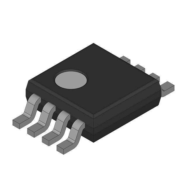
ADSANTEC ASNT8052-PQB

| Quantity | Unit Price | Total Price |
|---|---|---|
| 1 | $237.50 | $237.50 |
| 15+ | $230.00 | $3,450.00 |
| 25+ | $225.00 | $5,625.00 |
| 50+ | $212.50 | $10,625.00 |
| 100+ | $187.50 | $18,750.00 |
| N+ | $37.50 | Price Inquiry |
Request Quote / Inquiry
| Product attributes | Property Value |
| Manufacturer | ADSANTEC |
| Product Series | |
| Packaging | Bulk | |
| Type | PLL Clock Multiplier |
| PLL | Yes with Bypass |
| Input | CML, LVDS |
| Output | CML, LVDS |
| Number of Circuits | 1 |
| Ratio - Input:Output | 1:1 |
| Differential - Input:Output | Yes/Yes |
| Frequency - Max | 14.4GHz |
| Divider/Multiplier | Yes/Yes |
| Voltage - Supply | 3.1V ~ 3.5V |
| Operating Temperature | -25°C ~ 85°C |
| Grade | - |
| Qualification | - |
| Mounting Type | Surface Mount |
| Package / Case | 40-VFQFN Exposed Pad |
| Supplier Device Package | 40-QFN (6x6) |
| ROHS |  |
The ASNT8052-PQB from ADSANTEC is a PLL Clock Multiplier with a bypassable PLL for versatile operation. It features 1 circuit and supports CML and LVDS inputs/outputs, delivering up to 14.4 GHz output frequency. The differential signaling ensures low jitter and high noise immunity. Operating from -25°C to 85°C in a 40-VFQFN package, it is ideal for 5G, satellite, and high-performance computing applications.
- Ultra-High Frequency: 14.4 GHz output for cutting-edge applications.
- PLL Bypass: Provides design flexibility for various clocking schemes.
- Differential I/O: CML/LVDS ensures robust signal integrity.
- Wide Temperature Range: -25°C to 85°C for diverse environments.
5G mmWave Infrastructure
The 14.4 GHz output frequency supports 5G mmWave base stations requiring precise clock generation for beamforming.
High-Performance Computing
For HPC clusters, this multiplier provides synchronized clocks for high-speed interconnects like InfiniBand.
Satellite Communication
Its high frequency and differential outputs ensure reliable timing for satellite transponders and ground stations.
Medical Imaging
High-end ultrasound and MRI systems use precise clocks for data acquisition; this device delivers the needed frequency.
Quantum Computing
Control electronics for quantum processors require ultra-stable clocks; the ASNT8052-PQB meets these demands.
Radar Systems
Phased-array radar benefits from the device's high-frequency clock multiplication for accurate signal processing.
- Q: What type of device is the ASNT8052-PQB?
- A: It is a PLL Clock Multiplier from ADSANTEC, designed for high-frequency clock multiplication.
- Q: Does it support PLL bypass?
- A: Yes, it has 'Yes with Bypass' PLL, allowing direct clock input when PLL is not needed.
- Q: What are the input and output types?
- A: Both input and output types are CML and LVDS, providing differential signaling for high-speed data integrity.
- Q: How many circuits does it have?
- A: It has 1 circuit for clock multiplication.
- Q: What is the maximum frequency?
- A: The maximum frequency is 14.4 GHz, suitable for ultra-high-speed applications.
- Q: What is the operating temperature and package?
- A: It operates from -25°C to 85°C and comes in a 40-VFQFN Exposed Pad package.
 ASNT8052-PQB.pdf
- Q: What type of device is the ASNT8052-PQB?
- A: It is a PLL Clock Multiplier from ADSANTEC, designed for high-frequency clock multiplication.
- Q: Does it support PLL bypass?
- A: Yes, it has 'Yes with Bypass' PLL, allowing direct clock input when PLL is not needed.
- Q: What are the input and output types?
- A: Both input and output types are CML and LVDS, providing differential signaling for high-speed data integrity.
- Q: How many circuits does it have?
- A: It has 1 circuit for clock multiplication.
- Q: What is the maximum frequency?
- A: The maximum frequency is 14.4 GHz, suitable for ultra-high-speed applications.
- Q: What is the operating temperature and package?
- A: It operates from -25°C to 85°C and comes in a 40-VFQFN Exposed Pad package.