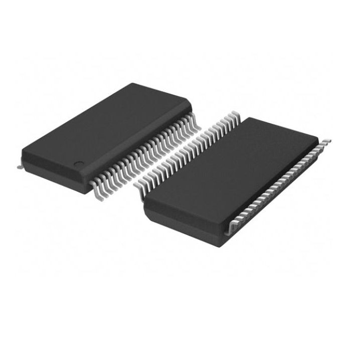
Texas Instruments CDC516DGGR

| Quantity | Unit Price | Total Price |
|---|---|---|
| 1 | $12.09 | $12.09 |
| 15+ | $11.71 | $175.65 |
| 25+ | $11.46 | $286.50 |
| 50+ | $10.82 | $541.00 |
| 100+ | $9.55 | $955.00 |
| N+ | $1.91 | Price Inquiry |
Request Quote / Inquiry
| Product attributes | Property Value |
| Manufacturer | Texas Instruments |
| Product Series | |
| Packaging | Marketplace | Cut Tape (CT) |
| Type | PLL Clock Driver |
| PLL | Yes with Bypass |
| Input | LVTTL |
| Output | LVTTL |
| Number of Circuits | 1 |
| Ratio - Input:Output | 1:16 |
| Differential - Input:Output | No/No |
| Frequency - Max | 125MHz |
| Divider/Multiplier | No/No |
| Voltage - Supply | 3V ~ 3.6V |
| Operating Temperature | 0°C ~ 70°C |
| Grade | - |
| Qualification | - |
| Mounting Type | Surface Mount |
| Package / Case | 48-TFSOP (0.240", 6.10mm Width) |
| Supplier Device Package | 48-TSSOP |
| ROHS |  |
The Texas Instruments CDC516DGGR is a PLL Clock Driver designed for reliable clock distribution in digital systems. It features a PLL with bypass capability, accepting LVTTL inputs and providing LVTTL outputs. With a single circuit supporting frequencies up to 125MHz, this device is well-suited for memory, networking, and embedded applications. Its 48-TFSOP package and 0°C to 70°C operating range make it a practical choice for commercial electronics requiring robust clock buffering and distribution.
- Low-Jitter Clock Distribution: Ensures clean, synchronized clocks for high-speed digital circuits, reducing timing errors.
- PLL Bypass Option: Offers flexibility to use the device as a simple buffer, simplifying design in non-PLL applications.
- LVTTL Compatibility: Works seamlessly with standard 3.3V logic, easing integration with existing designs.
- Compact TFSOP Package: Saves board space while providing adequate pin spacing for manufacturing.
Memory Clock Distribution
The CDC516DGGR is ideal for distributing clocks to DDR, DDR2, and DDR3 memory modules in servers and workstations, ensuring synchronized operation.
Networking Switch Timing
In Ethernet switches and routers, this clock driver provides clean, buffered clocks to PHYs, MACs, and switch fabrics, improving data throughput.
Embedded Processor Systems
For microprocessors and microcontrollers in industrial control systems, the device delivers stable clock signals to multiple peripherals and interfaces.
Telecom Line Cards
In telecom equipment, the CDC516DGGR distributes timing signals to line interface units and framers, maintaining network synchronization.
Consumer Electronics
Used in set-top boxes, gaming consoles, and digital TVs to distribute clocks to audio/video processors and interface chips.
- Q: What type of device is the CDC516DGGR?
- A: It is a PLL Clock Driver from Texas Instruments, designed to distribute and drive clock signals.
- Q: Does the CDC516DGGR have a PLL with bypass?
- A: Yes, it includes a PLL with bypass capability, allowing direct clock distribution when PLL is not needed.
- Q: What are the input and output types?
- A: Both input and output types are LVTTL (Low-Voltage TTL), making it compatible with standard digital logic.
- Q: How many circuits does it have and what is the maximum frequency?
- A: It has 1 circuit and supports a maximum frequency of 125MHz.
- Q: What is the operating temperature range?
- A: The operating temperature range is 0°C to 70°C.
- Q: What package is the CDC516DGGR available in?
- A: It is available in a 48-TFSOP package with a width of 6.10mm.
 CDC516DGGR.pdf
- Q: What type of device is the CDC516DGGR?
- A: It is a PLL Clock Driver from Texas Instruments, designed to distribute and drive clock signals.
- Q: Does the CDC516DGGR have a PLL with bypass?
- A: Yes, it includes a PLL with bypass capability, allowing direct clock distribution when PLL is not needed.
- Q: What are the input and output types?
- A: Both input and output types are LVTTL (Low-Voltage TTL), making it compatible with standard digital logic.
- Q: How many circuits does it have and what is the maximum frequency?
- A: It has 1 circuit and supports a maximum frequency of 125MHz.
- Q: What is the operating temperature range?
- A: The operating temperature range is 0°C to 70°C.
- Q: What package is the CDC516DGGR available in?
- A: It is available in a 48-TFSOP package with a width of 6.10mm.