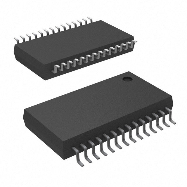
Texas Instruments CDC536DBR

| Quantity | Unit Price | Total Price |
|---|---|---|
| 1 | $22.82 | $22.82 |
| 15+ | $5.24 | $78.60 |
| 25+ | $5.13 | $128.25 |
| 50+ | $4.85 | $242.50 |
| 100+ | $4.28 | $428.00 |
| N+ | $0.86 | Price Inquiry |
Request Quote / Inquiry
| Product attributes | Property Value |
| Manufacturer | Texas Instruments |
| Product Series | |
| Packaging | Marketplace | Tape & Reel (TR) |
| Type | PLL Clock Driver |
| PLL | Yes with Bypass |
| Input | TTL |
| Output | LVTTL |
| Number of Circuits | 1 |
| Ratio - Input:Output | 1:6 |
| Differential - Input:Output | No/No |
| Frequency - Max | 100MHz |
| Divider/Multiplier | Yes/Yes |
| Voltage - Supply | 3V ~ 3.6V |
| Operating Temperature | 0°C ~ 70°C |
| Grade | - |
| Qualification | - |
| Mounting Type | Surface Mount |
| Package / Case | 28-SSOP (0.209", 5.30mm Width) |
| Supplier Device Package | 28-SSOP |
| ROHS |  |
The Texas Instruments CDC536DBR is a PLL Clock Driver designed for high-performance timing applications. It integrates a single PLL with bypass capability, accepting TTL inputs and delivering LVTTL outputs at frequencies up to 100MHz. Housed in a compact 28-SSOP package, this device is ideal for telecom, networking, and industrial systems requiring reliable clock generation and distribution.
- Flexible PLL with Bypass: Allows direct or synthesized clock paths, enabling designers to optimize for jitter or frequency accuracy.
- Single-Circuit Simplicity: Reduces board complexity and cost for applications needing one clean clock output.
- Wide Temperature Range: Operates from 0°C to 70°C, suitable for commercial and industrial environments.
- Standard LVTTL Interface: Ensures compatibility with common logic families, simplifying integration.
Telecom Clock Distribution
Use the CDC536DBR to distribute low-skew LVTTL clocks in telecom infrastructure, ensuring reliable timing for line cards and switching fabrics.
Networking Timing
Generate and buffer clocks for Ethernet switches and routers, maintaining synchronization across multiple ports with its PLL bypass feature for flexible timing paths.
Processor Clock Generation
Provide a clean 100MHz LVTTL clock to microprocessors and FPGAs in embedded systems, leveraging the PLL to reduce jitter and meet processor timing requirements.
Industrial Control Timing
Drive synchronous industrial controllers and PLCs with a stable TTL-to-LVTTL clock, ensuring precise operation in 0°C to 70°C environments.
Test and Measurement Equipment
Use the CDC536DBR in benchtop instruments to generate reference clocks for signal acquisition and generation, benefiting from its single-circuit simplicity and 100MHz capability.
- Q: What type of device is the CDC536DBR?
- A: It is a PLL Clock Driver from Texas Instruments.
- Q: Does the CDC536DBR support PLL?
- A: Yes, it has a PLL with bypass capability.
- Q: What are the input and output types?
- A: The input type is TTL and the output type is LVTTL.
- Q: How many circuits does it have?
- A: It has 1 circuit.
- Q: What is the maximum frequency?
- A: The maximum frequency is 100MHz.
- Q: What is the operating temperature and package?
- A: It operates from 0°C to 70°C and comes in a 28-SSOP package.
 CDC536DBR.pdf
- Q: What type of device is the CDC536DBR?
- A: It is a PLL Clock Driver from Texas Instruments.
- Q: Does the CDC536DBR support PLL?
- A: Yes, it has a PLL with bypass capability.
- Q: What are the input and output types?
- A: The input type is TTL and the output type is LVTTL.
- Q: How many circuits does it have?
- A: It has 1 circuit.
- Q: What is the maximum frequency?
- A: The maximum frequency is 100MHz.
- Q: What is the operating temperature and package?
- A: It operates from 0°C to 70°C and comes in a 28-SSOP package.