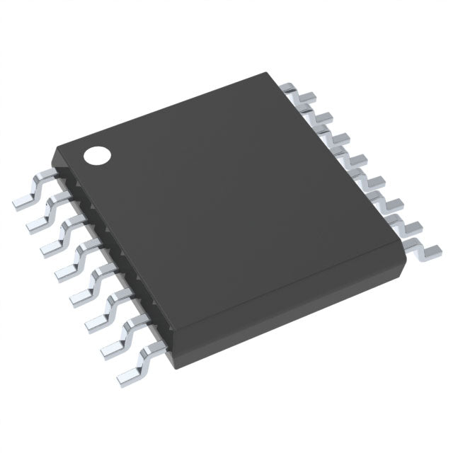
Texas Instruments CDCVF25084PW

| Quantity | Unit Price | Total Price |
|---|---|---|
| 1 | $27.37 | $27.37 |
| 15+ | $6.29 | $94.35 |
| 25+ | $6.16 | $154.00 |
| 50+ | $5.81 | $290.50 |
| 100+ | $5.13 | $513.00 |
| N+ | $1.03 | Price Inquiry |
Request Quote / Inquiry
| Product attributes | Property Value |
| Manufacturer | Texas Instruments |
| Product Series | |
| Packaging | Marketplace | Tube |
| Type | PLL Clock Multiplier |
| PLL | Yes with Bypass |
| Input | LVTTL |
| Output | LVTTL |
| Number of Circuits | 1 |
| Ratio - Input:Output | 2:8 |
| Differential - Input:Output | No/No |
| Frequency - Max | 180MHz |
| Divider/Multiplier | No/Yes |
| Voltage - Supply | 3V ~ 3.6V |
| Operating Temperature | -40°C ~ 85°C |
| Grade | - |
| Qualification | - |
| Mounting Type | Surface Mount |
| Package / Case | 16-TSSOP (0.173", 4.40mm Width) |
| Supplier Device Package | 16-TSSOP |
| ROHS |  |
The Texas Instruments CDCVF25084PW is a versatile PLL Clock Multiplier designed to generate higher-frequency clocks from a lower-frequency reference. It includes a PLL with bypass capability, allowing for flexible operation. With LVTTL inputs and outputs, this single-circuit device supports frequencies up to 180 MHz. It is ideal for processor, memory, and networking applications. It operates from -40°C to 85°C and is available in a 16-TSSOP package.
- PLL with Bypass: Provides flexibility to use the PLL for multiplication or bypass it for direct clock distribution.
- High Frequency: Supports up to 180 MHz, suitable for a wide range of digital systems.
- Wide Temperature Range: Operates from -40°C to 85°C, making it suitable for industrial environments.
- Compact TSSOP Package: Saves board space and is easy to integrate into existing designs.
Processor Clock Multiplication
The CDCVF25084PW can multiply a low-frequency reference clock to generate a higher-frequency clock for microprocessors and DSPs, improving system performance.
Memory Interface Timing
In DDR memory systems, this PLL multiplier can generate the required high-speed clock from a lower-frequency system clock, ensuring reliable data transfer.
Networking Equipment
For networking switches and routers, the CDCVF25084PW provides a clean, multiplied clock for PHYs and MACs, enhancing data throughput.
Consumer Electronics
In set-top boxes and gaming consoles, this device can generate the necessary clocks for video and audio processing, ensuring smooth operation.
Industrial Control
Its wide temperature range makes it suitable for industrial applications where a stable, multiplied clock is needed for PLCs and motor controllers.
FPGA Clock Generation
For FPGAs, this PLL multiplier can generate a high-frequency internal clock from an external reference, enabling complex logic designs.
- Q: What type of device is the CDCVF25084PW?
- A: It is a PLL Clock Multiplier from Texas Instruments.
- Q: Does it include a PLL?
- A: Yes, it includes a PLL with bypass capability.
- Q: What are the input and output types?
- A: It accepts LVTTL inputs and provides LVTTL outputs.
- Q: How many circuits does it have?
- A: It has 1 circuit.
- Q: What is the maximum frequency?
- A: The maximum frequency is 180 MHz.
- Q: What is the operating temperature and package?
- A: It operates from -40°C to 85°C and comes in a 16-TSSOP package.
 CDCVF25084PW.pdf
- Q: What type of device is the CDCVF25084PW?
- A: It is a PLL Clock Multiplier from Texas Instruments.
- Q: Does it include a PLL?
- A: Yes, it includes a PLL with bypass capability.
- Q: What are the input and output types?
- A: It accepts LVTTL inputs and provides LVTTL outputs.
- Q: How many circuits does it have?
- A: It has 1 circuit.
- Q: What is the maximum frequency?
- A: The maximum frequency is 180 MHz.
- Q: What is the operating temperature and package?
- A: It operates from -40°C to 85°C and comes in a 16-TSSOP package.