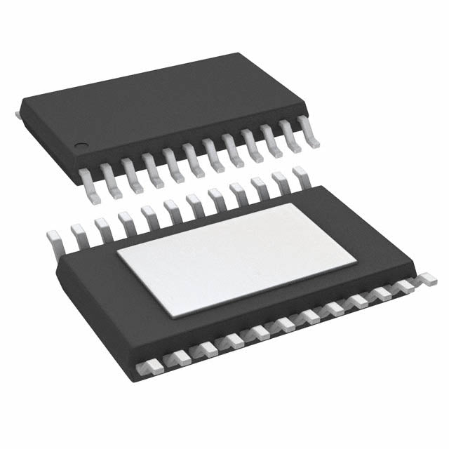
Texas Instruments CDCVF2509PWR

| Quantity | Unit Price | Total Price |
|---|---|---|
| 1 | $10.38 | $10.38 |
| 15+ | $10.06 | $150.90 |
| 25+ | $9.84 | $246.00 |
| 50+ | $9.29 | $464.50 |
| 100+ | $8.20 | $820.00 |
| N+ | $1.64 | Price Inquiry |
Request Quote / Inquiry
| Product attributes | Property Value |
| Manufacturer | Texas Instruments |
| Product Series | |
| Packaging | Marketplace | Cut Tape (CT) |
| Type | PLL Clock Driver |
| PLL | Yes with Bypass |
| Input | LVTTL |
| Output | LVTTL |
| Number of Circuits | 1 |
| Ratio - Input:Output | 2:10 |
| Differential - Input:Output | No/No |
| Frequency - Max | 175MHz |
| Divider/Multiplier | No/No |
| Voltage - Supply | 3V ~ 3.6V |
| Operating Temperature | 0°C ~ 85°C |
| Grade | - |
| Qualification | - |
| Mounting Type | Surface Mount |
| Package / Case | 24-TSSOP (0.173", 4.40mm Width) |
| Supplier Device Package | 24-TSSOP |
| ROHS |  |
The CDCVF2509PWR from Texas Instruments is a PLL Clock Driver designed for high-performance clock distribution. Featuring a PLL with bypass mode, it accepts LVTTL input and provides LVTTL outputs at frequencies up to 175MHz. With a single circuit and 0°C to 85°C operating range, this device is well-suited for DDR memory systems, networking equipment, and server platforms. The compact 24-TSSOP package makes it easy to integrate into space-constrained designs.
- PLL with Bypass: Provides flexibility to either synchronize outputs or bypass the PLL for direct clock distribution.
- High Frequency Operation: Supports up to 175MHz, making it suitable for DDR memory and high-speed networking.
- LVTTL Compatibility: Directly interfaces with standard 3.3V TTL logic without level shifting.
- Compact TSSOP Package: The 24-pin TSSOP package minimizes PCB footprint while providing adequate thermal performance.
DDR Memory Systems
The CDCVF2509PWR is ideal for generating and distributing clocks for DDR/DDR2/DDR3 memory modules, where precise timing alignment between the controller and DRAM is critical for data integrity.
Networking Switches
Use the CDCVF2509 to fan out reference clocks to multiple PHY devices and MAC controllers in Ethernet switches, ensuring synchronized operation across all ports.
Server Motherboards
In server platforms, this PLL clock driver provides clean, low-jitter clocks to the chipset, CPU, and I/O hubs, maintaining system stability under heavy load.
Telecom Line Cards
The device can distribute frame sync and line clocks in telecom line cards, supporting T1/E1 and SONET/SDH interfaces with its 175MHz capability.
Graphics and Video Processing
For graphics cards and video processing units, the CDCVF2509 ensures pixel clocks are distributed with minimal skew to multiple processing engines.
- Q: What type of device is the CDCVF2509PWR?
- A: It is a PLL Clock Driver from Texas Instruments, designed to distribute and synchronize clock signals in digital systems.
- Q: Does the CDCVF2509 include a PLL?
- A: Yes, it includes a PLL with bypass capability, allowing the device to either synchronize outputs to the input or pass the input directly to outputs.
- Q: What are the input and output types?
- A: Both input and output are LVTTL, making it compatible with standard 3.3V TTL logic.
- Q: How many circuits does it have and what is the maximum frequency?
- A: It has 1 circuit and supports a maximum frequency of 175MHz.
- Q: What is the operating temperature range?
- A: The CDCVF2509PWR operates from 0°C to 85°C, suitable for commercial applications.
- Q: What package is available?
- A: It is available in a 24-TSSOP package with 0.173" (4.40mm) width.
 CDCVF2509PWR.pdf
- Q: What type of device is the CDCVF2509PWR?
- A: It is a PLL Clock Driver from Texas Instruments, designed to distribute and synchronize clock signals in digital systems.
- Q: Does the CDCVF2509 include a PLL?
- A: Yes, it includes a PLL with bypass capability, allowing the device to either synchronize outputs to the input or pass the input directly to outputs.
- Q: What are the input and output types?
- A: Both input and output are LVTTL, making it compatible with standard 3.3V TTL logic.
- Q: How many circuits does it have and what is the maximum frequency?
- A: It has 1 circuit and supports a maximum frequency of 175MHz.
- Q: What is the operating temperature range?
- A: The CDCVF2509PWR operates from 0°C to 85°C, suitable for commercial applications.
- Q: What package is available?
- A: It is available in a 24-TSSOP package with 0.173" (4.40mm) width.