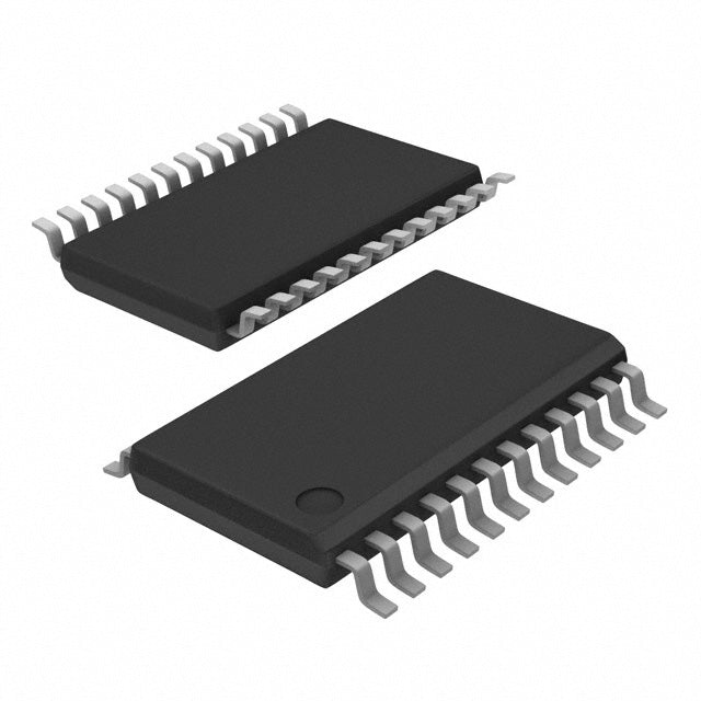
Texas Instruments CDCVF2510APW

| Quantity | Unit Price | Total Price |
|---|---|---|
| 1 | $5.18 | $5.18 |
| 15+ | $5.01 | $75.15 |
| 25+ | $4.91 | $122.75 |
| 50+ | $4.63 | $231.50 |
| 100+ | $4.09 | $409.00 |
| N+ | $0.82 | Price Inquiry |
Request Quote / Inquiry
| Product attributes | Property Value |
| Manufacturer | Texas Instruments |
| Product Series | |
| Packaging | Marketplace | Tube |
| Type | PLL Clock Driver |
| PLL | Yes with Bypass |
| Input | LVTTL |
| Output | LVTTL |
| Number of Circuits | 1 |
| Ratio - Input:Output | 2:11 |
| Differential - Input:Output | No/No |
| Frequency - Max | 175MHz |
| Divider/Multiplier | No/No |
| Voltage - Supply | 3V ~ 3.6V |
| Operating Temperature | 0°C ~ 85°C |
| Grade | - |
| Qualification | - |
| Mounting Type | Surface Mount |
| Package / Case | 24-TSSOP (0.173", 4.40mm Width) |
| Supplier Device Package | 24-TSSOP |
| ROHS |  |
The Texas Instruments CDCVF2510APW is a PLL Clock Driver designed for high-performance clock distribution. It features a PLL with bypass and accepts LVTTL inputs, providing LVTTL outputs up to 175MHz. This single-circuit device in a 24-pin TSSOP package is ideal for DDR memory systems, computing platforms, and networking equipment requiring low-skew, synchronized clocks.
- Low Output Skew: Ensures synchronized clock distribution to multiple loads, critical for high-speed memory and logic interfaces.
- PLL with Bypass: Provides flexibility for frequency multiplication or direct clock buffering.
- Standard LVTTL Interface: Compatible with a wide range of digital logic families, simplifying design.
- High Frequency Support: Operates up to 175MHz, suitable for DDR and high-speed logic.
DDR Memory Clock Distribution
Use the CDCVF2510APW to distribute low-skew clocks to DDR SDRAM devices. The PLL ensures precise alignment between the command/address and data clocks.
High-Performance Computing
Provide clean, buffered clocks to multiple processors, memory controllers, and I/O hubs in servers and workstations. The LVTTL outputs are compatible with standard logic families.
Networking and Storage Systems
Generate and distribute clocks for network processors, switch fabrics, and storage controllers. The PLL with bypass allows for both frequency multiplication and direct buffering.
Telecom Line Cards
Distribute timing signals to multiple line interface units (LIUs) and framers. The low output skew ensures synchronized operation across the line card.
Test and Measurement Equipment
Use in ATE and lab instruments to provide multiple synchronized clock signals for testing high-speed digital devices.
- Q: What type of device is the CDCVF2510APW?
- A: It is a PLL Clock Driver from Texas Instruments.
- Q: Does it have a PLL?
- A: Yes, it has a PLL with bypass capability.
- Q: What are the input and output types?
- A: Both input and output types are LVTTL.
- Q: How many circuits does it have and what is the max frequency?
- A: It has 1 circuit and supports up to 175MHz.
- Q: What is the operating temperature range?
- A: 0°C to 85°C.
- Q: What is the package type?
- A: 24-TSSOP (0.173", 4.40mm Width).
 CDCVF2510APW.pdf
- Q: What type of device is the CDCVF2510APW?
- A: It is a PLL Clock Driver from Texas Instruments.
- Q: Does it have a PLL?
- A: Yes, it has a PLL with bypass capability.
- Q: What are the input and output types?
- A: Both input and output types are LVTTL.
- Q: How many circuits does it have and what is the max frequency?
- A: It has 1 circuit and supports up to 175MHz.
- Q: What is the operating temperature range?
- A: 0°C to 85°C.
- Q: What is the package type?
- A: 24-TSSOP (0.173", 4.40mm Width).