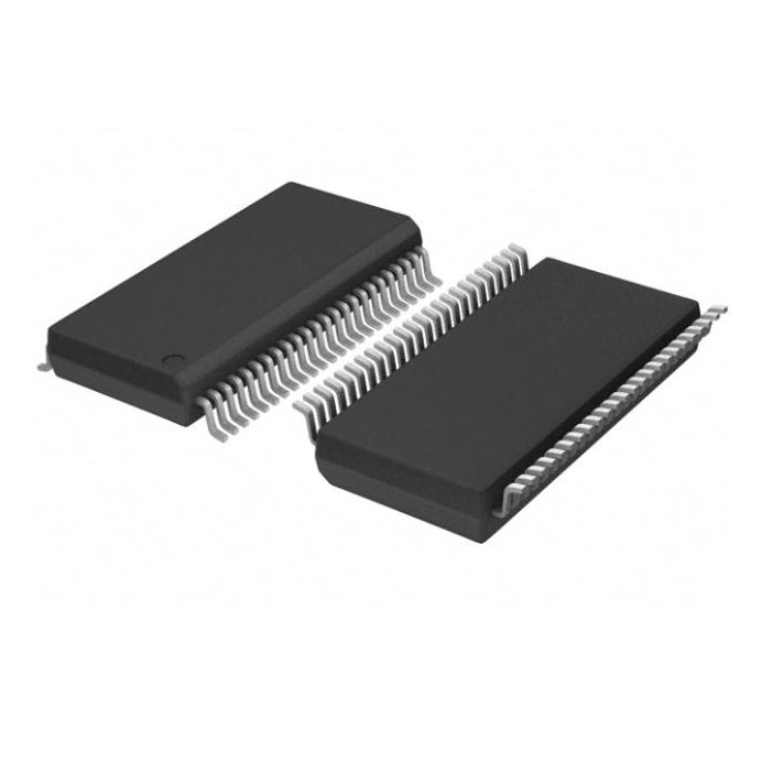
Texas Instruments CDCVF857DGGR

| Quantity | Unit Price | Total Price |
|---|---|---|
| 1 | $8.18 | $8.18 |
| 15+ | $7.92 | $118.80 |
| 25+ | $7.75 | $193.75 |
| 50+ | $7.32 | $366.00 |
| 100+ | $6.46 | $646.00 |
| N+ | $1.29 | Price Inquiry |
Request Quote / Inquiry
| Product attributes | Property Value |
| Manufacturer | Texas Instruments |
| Product Series | |
| Packaging | Marketplace | Cut Tape (CT) |
| Type | PLL Clock Driver |
| PLL | Yes with Bypass |
| Input | SSTL-2 |
| Output | SSTL-2 |
| Number of Circuits | 1 |
| Ratio - Input:Output | 2:11 |
| Differential - Input:Output | Yes/Yes |
| Frequency - Max | 220MHz |
| Divider/Multiplier | No/No |
| Voltage - Supply | 2.3V ~ 2.7V |
| Operating Temperature | -40°C ~ 85°C |
| Grade | - |
| Qualification | - |
| Mounting Type | Surface Mount |
| Package / Case | 48-TFSOP (0.240", 6.10mm Width) |
| Supplier Device Package | 48-TSSOP |
| ROHS |  |
The CDCVF857DGGR is a PLL Clock Driver from Texas Instruments, designed for high-performance clock distribution in DDR memory and computing applications. It features a PLL with bypass capability, allowing flexible operation as a zero-delay buffer or direct clock driver. Supporting up to 220 MHz with SSTL-2 differential signaling, this device ensures low skew and high noise immunity. Its single circuit and industrial temperature range make it a robust choice for servers, networking, and industrial systems requiring precise timing.
- PLL with Bypass: Offers flexibility to use the PLL for zero-delay buffering or bypass it for direct distribution, adapting to various system requirements.
- Differential SSTL-2 Interface: Provides superior noise immunity and signal integrity for high-speed DDR memory applications.
- Industrial Temperature Range: Operates from -40°C to 85°C, ensuring reliable performance in demanding environments.
- High-Frequency Support: Handles up to 220 MHz, meeting the clocking needs of modern DDR memory and high-speed digital systems.
DDR Memory Clock Distribution
Generate and distribute precise clock signals for DDR/DDR2 memory modules, using the SSTL-2 interface and PLL to minimize skew and ensure reliable data capture.
Server and Workstation Motherboards
Provide low-jitter clock distribution for CPU and memory subsystems in high-performance servers, where timing accuracy is critical for system stability.
Networking Switch Timing
Synchronize packet processing and switching operations in network equipment, leveraging the PLL to align clocks across multiple line cards.
Telecom Line Cards
Distribute reference clocks to multiple transceivers and framers on telecom line cards, ensuring coherent operation and reducing bit errors.
Graphics Card Memory Interface
Clock the graphics memory interface in GPUs, using the high-frequency capability and differential SSTL-2 signaling to support high-bandwidth data transfer.
Industrial Computing Systems
Provide reliable clock distribution in industrial PCs and embedded systems, where the wide temperature range ensures operation in harsh environments.
- Q: What type of device is the CDCVF857DGGR?
- A: It is a PLL Clock Driver from Texas Instruments, designed to distribute and buffer clock signals with low skew.
- Q: Does the CDCVF857DGGR support PLL bypass?
- A: Yes, it features 'Yes with Bypass', meaning the PLL can be enabled for zero-delay buffering or bypassed for direct clock distribution.
- Q: What are the input and output types?
- A: Both input and output are SSTL-2, a differential signaling standard used in DDR memory systems. This provides high noise immunity.
- Q: How many circuits does it have and what is the maximum frequency?
- A: It has 1 circuit and supports a maximum frequency of 220 MHz, suitable for DDR memory clocking.
- Q: What is the operating temperature range?
- A: The device operates over an industrial temperature range of -40°C to 85°C.
- Q: What package is the CDCVF857DGGR available in?
- A: It comes in a 48-TFSOP package with a width of 6.10mm.
 CDCVF857DGGR.pdf
- Q: What type of device is the CDCVF857DGGR?
- A: It is a PLL Clock Driver from Texas Instruments, designed to distribute and buffer clock signals with low skew.
- Q: Does the CDCVF857DGGR support PLL bypass?
- A: Yes, it features 'Yes with Bypass', meaning the PLL can be enabled for zero-delay buffering or bypassed for direct clock distribution.
- Q: What are the input and output types?
- A: Both input and output are SSTL-2, a differential signaling standard used in DDR memory systems. This provides high noise immunity.
- Q: How many circuits does it have and what is the maximum frequency?
- A: It has 1 circuit and supports a maximum frequency of 220 MHz, suitable for DDR memory clocking.
- Q: What is the operating temperature range?
- A: The device operates over an industrial temperature range of -40°C to 85°C.
- Q: What package is the CDCVF857DGGR available in?
- A: It comes in a 48-TFSOP package with a width of 6.10mm.