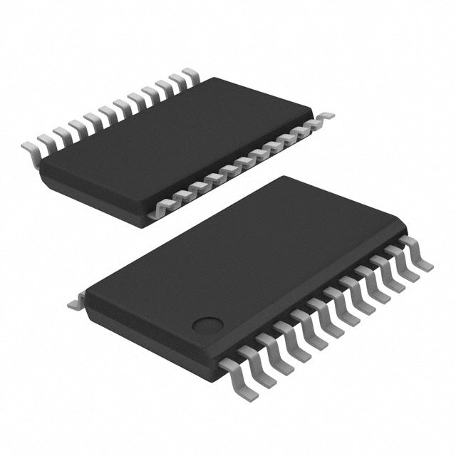
Texas Instruments SN74AXC8T245QPWRQ1

| Quantity | Unit Price | Total Price |
|---|---|---|
| 1 | $1.48 | $1.48 |
| 15+ | $1.44 | $21.60 |
| 25+ | $1.40 | $35.00 |
| 50+ | $1.33 | $66.50 |
| 100+ | $1.17 | $117.00 |
| N+ | $0.23 | Price Inquiry |
Request Quote / Inquiry
| Product attributes | Property Value |
| Manufacturer | Texas Instruments |
| Product Series | 74AXC |
| Packaging | Cut Tape (CT) | Tape & Reel (TR) |
| Part Status | Active |
| Logic Type | Translation Transceiver |
| Number of Elements | 1 |
| Number of Bits per Element | 8 |
| Input Type | - |
| Output Type | Tri-State, Non-Inverted |
| Current - Output High, Low | 12mA, 12mA |
| Voltage - Supply | 0.65V ~ 3.6V |
| Operating Temperature | -40°C ~ 125°C (TA) |
| Grade | Automotive |
| Qualification | AEC-Q100 |
| Mounting Type | Surface Mount |
| Package / Case | 24-TSSOP (0.173", 4.40mm Width) |
| Supplier Device Package | 24-TSSOP |
| ROHS |  |
The SN74AXC8T245QPWRQ1 from Texas Instruments is an automotive-grade 8-bit translation transceiver designed for ultra-low-voltage level shifting. Operating from 0.65V to 3.6V, it supports the latest low-voltage processors and FPGAs while interfacing with standard 1.8V and 3.3V logic. With tri-state, non-inverted outputs and 12mA drive capability, it ensures reliable bidirectional data transfer. Housed in a 24-TSSOP package, this 74AXC family device is ideal for automotive ADAS, IoT edge nodes, and portable medical devices.
- Ultra-Low Voltage Operation (0.65V-3.6V): Compatible with the latest low-voltage processors and FPGAs.
- Automotive Qualified (AEC-Q100): Reliable operation from -40°C to 125°C for harsh environments.
- Bidirectional Translation: Supports both step-up and step-down level shifting in one device.
- Tri-State Outputs: Allows bus isolation and prevents contention in multi-device systems.
- High-Speed Performance: Supports fast data rates for modern digital interfaces.
Ultra-Low-Voltage Processor Interfacing
Modern processors operate at 0.8V or 1.0V core voltages. The SN74AXC8T245QPWRQ1 translates these ultra-low signals to 1.8V or 3.3V for peripherals, enabling seamless communication with standard logic.
FPGA Configuration and I/O Expansion
FPGAs often have multiple I/O banks at different voltages. This transceiver provides bidirectional level shifting between banks, allowing flexible I/O assignment and simplifying PCB routing.
Automotive ADAS Sensor Fusion
In ADAS systems, cameras and radar sensors output data at various voltage levels. This AEC-Q100 qualified device translates signals between sensor modules and the central processing unit, ensuring reliable data fusion.
Portable Medical Devices
Battery-powered medical monitors use low-voltage sensors and microcontrollers. This transceiver enables efficient level shifting with minimal power draw, extending battery life while maintaining signal integrity.
IoT Edge Node Communication
IoT devices combine low-power MCUs (0.9V) with wireless modules (1.8V or 3.3V). This device provides the necessary voltage translation for reliable data exchange in smart home and industrial IoT applications.
High-Speed Data Acquisition
In data acquisition systems, ADCs and DACs operate at different voltage levels. This transceiver supports high-speed bidirectional data flow, preserving signal integrity for accurate measurements.
- Q: What logic family does the SN74AXC8T245QPWRQ1 use?
- A: It is from the 74AXC family, designed for ultra-low-voltage and high-speed applications.
- Q: What is the function of this device?
- A: It is an 8-bit translation transceiver with tri-state, non-inverted outputs for bidirectional level shifting.
- Q: How many channels does it have?
- A: It has 1 channel with 8 bits, supporting 8-bit bidirectional data transfer.
- Q: What is the output type?
- A: The outputs are tri-state and non-inverted, allowing the device to be disabled while preserving signal polarity.
- Q: What is the voltage range?
- A: It operates from 0.65V to 3.6V, making it ideal for ultra-low-voltage processors and FPGAs.
- Q: What package is available?
- A: It is available in a 24-TSSOP package (0.173", 4.40mm width), suitable for compact automotive designs.
 SN74AXC8T245QPWRQ1.pdf
- Q: What logic family does the SN74AXC8T245QPWRQ1 use?
- A: It is from the 74AXC family, designed for ultra-low-voltage and high-speed applications.
- Q: What is the function of this device?
- A: It is an 8-bit translation transceiver with tri-state, non-inverted outputs for bidirectional level shifting.
- Q: How many channels does it have?
- A: It has 1 channel with 8 bits, supporting 8-bit bidirectional data transfer.
- Q: What is the output type?
- A: The outputs are tri-state and non-inverted, allowing the device to be disabled while preserving signal polarity.
- Q: What is the voltage range?
- A: It operates from 0.65V to 3.6V, making it ideal for ultra-low-voltage processors and FPGAs.
- Q: What package is available?
- A: It is available in a 24-TSSOP package (0.173", 4.40mm width), suitable for compact automotive designs.