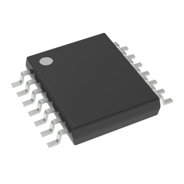
Texas Instruments SN74LVC125APWRG3

| Quantity | Unit Price | Total Price |
|---|---|---|
| 1 | $0.37 | $0.37 |
| 15+ | $0.36 | $5.40 |
| 25+ | $0.35 | $8.75 |
| 50+ | $0.33 | $16.50 |
| 100+ | $0.29 | $29.00 |
| N+ | $0.06 | Price Inquiry |
Request Quote / Inquiry
| Product attributes | Property Value |
| Manufacturer | Texas Instruments |
| Product Series | 74LVC |
| Packaging | Cut Tape (CT) | Tape & Reel (TR) |
| Part Status | Active |
| Logic Type | Buffer, Non-Inverting |
| Number of Elements | 4 |
| Number of Bits per Element | 1 |
| Input Type | - |
| Output Type | 3-State |
| Current - Output High, Low | 24mA, 24mA |
| Voltage - Supply | 1.65V ~ 3.6V |
| Operating Temperature | -40°C ~ 125°C (TA) |
| Grade | - |
| Qualification | - |
| Mounting Type | Surface Mount |
| Package / Case | 14-TSSOP (0.173", 4.40mm Width) |
| Supplier Device Package | 14-TSSOP |
| ROHS |  |
The SN74LVC125APWRG3 is a quad non-inverting buffer from Texas Instruments' 74LVC family. It features four channels with 3-state outputs, providing flexible bus control and signal isolation. Operating from 1.65V to 3.6V, it supports low-voltage logic with ±24mA output drive. The compact 14-TSSOP package is ideal for space-constrained designs. Applications include bus interfacing, signal buffering, and level shifting in portable, automotive, and industrial electronics.
- Compact TSSOP Package: Saves board space compared to SOIC, ideal for high-density designs.
- Wide 1.65V to 3.6V Supply: Compatible with multiple low-voltage logic standards.
- 3-State Outputs: Enables bus sharing and prevents data corruption in multi-device systems.
- High 24mA Drive: Ensures robust signal integrity for demanding applications.
Compact Bus Interface for Portable Devices
The TSSOP package saves PCB space, making it ideal for smartphones and wearables where board area is limited. The 3-state outputs allow multiple peripherals to share a data bus efficiently.
Signal Buffering for FPGA I/O Expansion
Buffer FPGA output signals to drive multiple loads or longer traces. The 24mA drive strength ensures clean signal propagation, reducing reflections and maintaining timing margins.
Level Shifting in Mixed-Voltage Systems
With a 1.65V to 3.6V supply, this buffer can translate between 1.8V and 3.3V logic domains, enabling communication between low-power processors and standard peripherals.
Memory Address/Data Bus Isolation
Use the 3-state outputs to isolate memory banks during read/write cycles, preventing bus contention and improving system reliability in multi-bank memory designs.
Automotive Infotainment Systems
Rated for -40°C to 125°C, this buffer is suitable for automotive infotainment units, buffering signals between the main processor and display or audio modules.
Industrial Sensor Data Acquisition
Buffer analog-to-digital converter outputs to a microcontroller, ensuring stable data transfer in noisy industrial environments with the high noise immunity of the 74LVC family.
- Q: What is the logic family of the SN74LVC125APWRG3?
- A: It belongs to the 74LVC family, designed for low-voltage, high-speed logic applications.
- Q: What is the function of this IC?
- A: It is a quad (4-channel) non-inverting buffer with 3-state outputs, used for signal buffering and bus isolation.
- Q: How many channels does it have?
- A: It contains 4 independent buffer channels, each with its own output enable pin.
- Q: What is the output type?
- A: The outputs are 3-State, allowing high, low, or high-impedance states for bus sharing.
- Q: What is the operating voltage range?
- A: It operates from 1.65V to 3.6V, supporting 1.8V, 2.5V, and 3.3V logic levels.
- Q: What package is available?
- A: It comes in a 14-pin TSSOP package (0.173", 4.40mm width), offering a smaller footprint than SOIC.
 SN74LVC125APWRG3.pdf
- Q: What is the logic family of the SN74LVC125APWRG3?
- A: It belongs to the 74LVC family, designed for low-voltage, high-speed logic applications.
- Q: What is the function of this IC?
- A: It is a quad (4-channel) non-inverting buffer with 3-state outputs, used for signal buffering and bus isolation.
- Q: How many channels does it have?
- A: It contains 4 independent buffer channels, each with its own output enable pin.
- Q: What is the output type?
- A: The outputs are 3-State, allowing high, low, or high-impedance states for bus sharing.
- Q: What is the operating voltage range?
- A: It operates from 1.65V to 3.6V, supporting 1.8V, 2.5V, and 3.3V logic levels.
- Q: What package is available?
- A: It comes in a 14-pin TSSOP package (0.173", 4.40mm width), offering a smaller footprint than SOIC.